| CPC H01L 23/5384 (2013.01) [H01L 21/76802 (2013.01); H01L 21/76877 (2013.01); H01L 23/5386 (2013.01)] | 13 Claims |
|
1. A method of manufacturing a semiconductor structure, comprising:
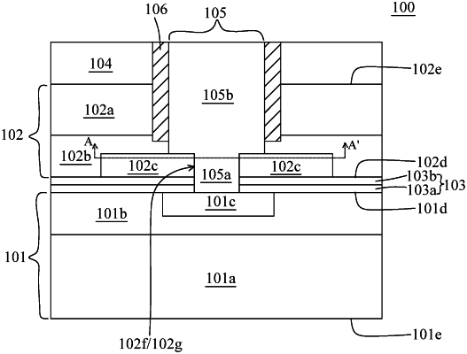
providing a first wafer including a first substrate, a first dielectric layer over the first substrate, and a first conductive pad surrounded by the first dielectric layer and recessed from a first surface of the first dielectric layer, wherein the first conductive pad is formed by removing a portion of the first dielectric layer to form a recess on the first surface of the first dielectric layer and filling a first conductive pad material in the recess, such that the conductive pad is recessed from the first surface of the first dielectric layer;
providing a second wafer including a second substrate, a second dielectric layer over the second substrate, and a second conductive pad surrounded by the second dielectric layer;
disposing a passivation over the second substrate;
bonding the first dielectric layer with the second dielectric layer by a bonding dielectric;
forming a first opening extending through the second substrate and partially through the second dielectric layer;
disposing a dielectric liner conformal to the first opening at a position that the dielectric liner is disposed between a conductive via and the second wafer, wherein the dielectric liner is disposed partially through the second dielectric layer, wherein a top surface of the dielectric liner is coplanar with a top surface of the passivation and a top surface of the conductive via; and
forming a second opening extending through the second dielectric layer and the second conductive pad to at least partially expose the first conductive pad;
wherein forming the conductive via over the conductive pad by disposing a conductive material within the first opening and the second opening by the steps of:
forming a first portion of the conductive via through the second opening to the first surface of the first dielectric layer at a position that the first portion of the conductive via is surrounded by the bonding dielectric and the second conductive pad and not exposed to the second dielectric layer; and
coupling a second portion of the conductive via with the first portion thereof at a position that the second portion of the conductive via is surrounded by the second dielectric layer and the second substrate, wherein the dielectric liner is sandwiched between the second portion of conductive via and the passivation.
|