| CPC H01L 23/5384 (2013.01) [H01L 23/31 (2013.01); H01L 23/5385 (2013.01); H01L 23/5386 (2013.01); H01L 25/0657 (2013.01)] | 18 Claims |
|
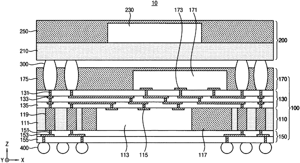
1. A semiconductor package comprising:
a first package comprising:
a first semiconductor chip;
a second semiconductor chip;
a core member including a through-hole penetrating the core member, wherein at least one of the first and second semiconductor chips is disposed in the through-hole;
an encapsulant disposed in the through-hole, and encapsulating the at least one of the first and second semiconductor chips disposed in the through-hole;
a first redistribution layer disposed above the core member, the first redistribution layer is electrically connected to the first and second semiconductor chips;
a second redistribution layer disposed under the core member, the second redistribution layer is configured to electrically connect the first and second semiconductor chips with an external printed circuit board (PCB); and
core vias penetrating the core member, the core vias are configured to electrically connect the first redistribution layer with the second redistribution layer;
a second package disposed on the first package, the second package including a third semiconductor chip;
a plurality of first electrical connection structures disposed between the first package and the second package, the plurality of first electrical connection structures is configured to electrically connect the first package with the second package, each of the plurality of first electrical connection structures directly contacts an upper surface of the first redistribution layer and the second package, wherein a lower surface of the plurality of first electrical connection structures is co-planar with a lower surface of the second semiconductor chip; and
a plurality of second electrical connection structures disposed under the first package, the plurality of second electrical connection structures is configured to electrically connect the semiconductor package with the external PCB.
|
|
17. A semiconductor package comprising:
a first package comprising:
a first semiconductor chip;
a second semiconductor chip;
a core member including a through-hole penetrating the core member, wherein the first semiconductor chip is disposed in the through-hole;
an encapsulant disposed in the through-hole, and encapsulating the at least one of the first and second semiconductor chips disposed in the through-hole;
a first redistribution layer disposed above the core member, the first redistribution layer is electrically connected to the first and second semiconductor chips, wherein the second semiconductor chip is disposed on the first redistribution layer;
a second redistribution layer disposed under the core member, the second redistribution layer is configured to electrically connect the first and second semiconductor chips with an external printed circuit board (PCB); and
core vias penetrating the core member, the core vias are configured to electrically connect the first redistribution layer with the second redistribution layer:
a second package disposed on the first package, the second package including a third semiconductor chip;
a plurality of first electrical connection structures disposed between the first package and the second package, the plurality of first electrical connection structures is configured to electrically connect the first package with the second package, each of the plurality of first electrical connection structures directly contacts an upper surface of the first redistribution layer and the second package; and
a plurality of second electrical connection structures disposed under the first package, the plurality of second electrical connection structures is configured to electrically connect the semiconductor package with the external PCB,
wherein the first package further includes:
a second encapsulant disposed on the first redistribution layer, and encapsulating the second semiconductor chip.
|