| CPC H01L 23/5283 (2013.01) [H01L 21/76816 (2013.01); H01L 21/76843 (2013.01); H01L 21/76879 (2013.01); H01L 23/5226 (2013.01); H01L 23/53223 (2013.01); H01L 23/53238 (2013.01); H01L 23/53252 (2013.01); H01L 23/53266 (2013.01)] | 20 Claims |
|
1. A semiconductor device comprising:
a transistor on a substrate;
a first metal layer on the transistor, the first metal layer comprising a lower interconnection line electrically connected to the transistor; and
a second metal layer on the first metal layer,
wherein the second metal layer comprises an upper interconnection line electrically connected to the lower interconnection line,
wherein the upper interconnection line comprises:
a via structure in a via hole; and
a line structure in a line trench,
wherein the via structure comprises:
a via portion that is in the via hole and is coupled to the lower interconnection line; and
a barrier portion that vertically extends from the via portion to cover an inner surface of the line trench,
wherein the barrier portion is between the line structure and an interlayer insulating layer of the second metal layer,
wherein the barrier portion has a first thickness at its upper level, and
wherein the barrier portion has a second thickness that is larger than the first thickness, at a level adjacent to the via portion.
|
|
11. A semiconductor device comprising:
a transistor on a substrate;
a first metal layer on the transistor, the first metal layer comprising a lower interconnection line electrically connected to the transistor; and
a second metal layer on the first metal layer,
wherein the second metal layer comprises an upper interconnection line electrically connected to the lower interconnection line,
wherein the upper interconnection line comprises:
a via structure in a via hole; and
a line structure in a line trench,
wherein the via structure comprises:
a via portion that is in the via hole and is coupled to the lower interconnection line; and
a barrier portion that vertically extends from the via portion to cover an inner surface of the line trench,
wherein the barrier portion is between the line structure and an interlayer insulating layer of the second metal layer, and
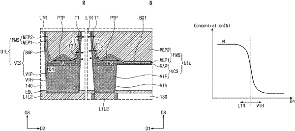
wherein a nitrogen concentration of the barrier portion is higher than a nitrogen concentration of the via portion.
|
|
16. A semiconductor device comprising:
a substrate including an active region;
a device isolation layer defining active patterns on the active region, the device isolation layer covering a lower side surface of each of the active patterns, an upper portion of each of the active patterns protruding above the device isolation layer;
a pair of source/drain patterns in an upper portion of each of the active patterns;
a channel pattern between the pair of source/drain patterns;
a gate electrode extending in a first direction to cross the channel pattern;
gate spacers on opposite side surfaces of the gate electrode and extending in the first direction along with the gate electrode;
a gate dielectric layer between the gate electrode and the channel pattern and between the gate electrode and the gate spacers;
a gate capping pattern that is on a top surface of the gate electrode and extends in the first direction along with the gate electrode;
a first interlayer insulating layer on the gate capping pattern;
an active contact that penetrates the first interlayer insulating layer and is electrically connected to at least one of the pair of source/drain patterns;
a first metal layer in a second interlayer insulating layer on the first interlayer insulating layer;
a second metal layer in a third interlayer insulating layer on the second interlayer insulating layer; and
an etch stop layer between the second interlayer insulating layer and the third interlayer insulating layer,
wherein the first metal layer comprises a lower interconnection line electrically connected to the active contact,
wherein the second metal layer comprises an upper interconnection line electrically connected to the lower interconnection line,
wherein the upper interconnection line comprises:
a via structure in a via hole; and
a line structure in a line trench,
wherein the via structure comprises:
a via portion that is in the via hole, penetrates the etch stop layer, and is coupled to the lower interconnection line; and
a barrier portion that vertically extends from the via portion to cover an inner surface of the line trench,
wherein the barrier portion is between the line structure and the third interlayer insulating layer, and
wherein the via portion and the barrier portion comprise the same metal and are integrated together as a single object.
|