| CPC H01L 23/5283 (2013.01) [H01L 23/5226 (2013.01); H01L 23/53209 (2013.01); H10B 43/35 (2023.02); H10B 43/40 (2023.02); H10B 41/35 (2023.02); H10B 41/40 (2023.02)] | 14 Claims |
|
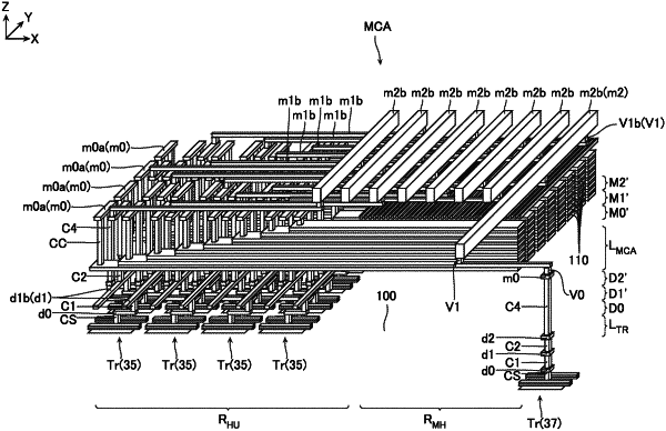
1. A semiconductor memory device comprising:
a semiconductor substrate;
a plurality of memory blocks spaced from the semiconductor substrate in a first direction intersecting with a surface of the semiconductor substrate, the plurality of memory blocks being arranged in a second direction intersecting with the first direction;
a first wiring that is farther from the semiconductor substrate than the plurality of memory blocks in the first direction;
a second wiring that is closer to the semiconductor substrate than the plurality of memory blocks in the first direction;
a first contact, the first wiring being electrically connected to the second wiring via the first contact;
a first transistor with a first active region disposed in the semiconductor substrate, the second wiring being electrically connected to a first memory block among the plurality of memory blocks via the first transistor; and
a second transistor with a second active region disposed in the semiconductor substrate, the second wiring being electrically connected to a second memory block among the plurality of memory blocks via the second transistor, wherein
the first contact is positioned between the first transistor and the second transistor in the second direction.
|