| CPC H01L 23/5228 (2013.01) [H01L 21/4846 (2013.01); H01L 21/76871 (2013.01); H01L 23/498 (2013.01); H01L 23/5226 (2013.01); H01L 23/647 (2013.01); H01L 24/09 (2013.01); H01L 27/016 (2013.01); H01L 28/24 (2013.01)] | 15 Claims |
|
1. A package substrate, comprising:
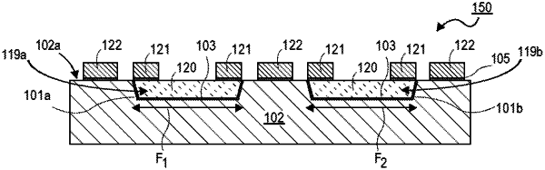
a dielectric having a first cavity and a second cavity, wherein the first cavity has a first footprint and the second cavity has a second footprint different than the first footprint;
a first resistor embedded in the first cavity of the dielectric and a second resistor embedded in the second cavity of the dielectric, wherein each of the first resistor and the second resistor has a plurality of surfaces and a top surface, and wherein a resistance value of the first resistor is different than a resistance value of the second resistor;
a plurality of first traces on the top surface of the first resistor and a plurality of second traces on the top surface of the second resistor, wherein the plurality of surfaces of the first resistor and the second resistor are a plurality of activated surfaces; and
a plurality of routing traces on the dielectric, wherein the plurality of routing traces are adjacent to the plurality of first traces and the plurality of second traces.
|