| CPC H01L 23/5226 (2013.01) [H01L 21/76807 (2013.01); H01L 21/76877 (2013.01)] | 20 Claims |
|
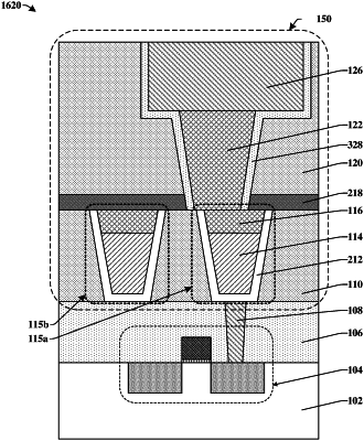
1. A method for forming an interconnect structure, the method comprising:
forming a first conductive material in a first opening in a first dielectric layer;
recessing the first conductive material below a top surface of the first dielectric layer;
forming a second conductive material in the first opening and over the first conductive material;
forming a second dielectric layer over the first dielectric layer;
forming a second opening in the second dielectric layer and over the second conductive material;
forming a third conductive material in the second opening; and
forming a fourth conductive material over the third conductive material,
wherein the second conductive material and the third conductive material have lower diffusion coefficients than the first conductive material and the fourth conductive material.
|