| CPC H01L 23/49838 (2013.01) [H01L 21/4853 (2013.01); H01L 21/4871 (2013.01); H01L 21/563 (2013.01); H01L 23/3185 (2013.01); H01L 23/3672 (2013.01); H01L 23/4985 (2013.01); H01L 24/16 (2013.01); H01L 2224/16227 (2013.01); H01L 2924/18161 (2013.01)] | 20 Claims |
|
1. A chip-on-film (CoF) package, comprising:
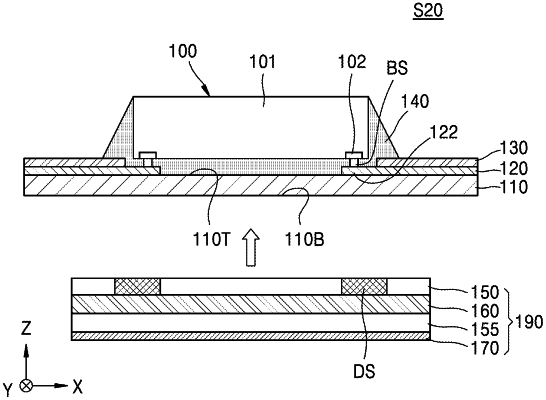
a base film having an upper surface and a lower surface facing each other;
a conductive line on the upper surface of the base film;
a semiconductor chip on the upper surface of the base film and connected to the conductive line through a bump structure;
a heat radiator on the lower surface of the base film and underlying the semiconductor chip;
an adhesive layer between the lower surface of the base film and the heat radiator; and
a plurality of dam structures in the adhesive layer and overlapping the bump structure,
wherein, in plan view, the plurality of dam structures are discontinuously arranged in an island shape.
|