| CPC H01L 23/49827 (2013.01) [H01L 21/486 (2013.01); H01L 23/49866 (2013.01); H05K 1/113 (2013.01); H05K 3/184 (2013.01); H05K 2201/0379 (2013.01); H05K 2203/0565 (2013.01)] | 6 Claims |
|
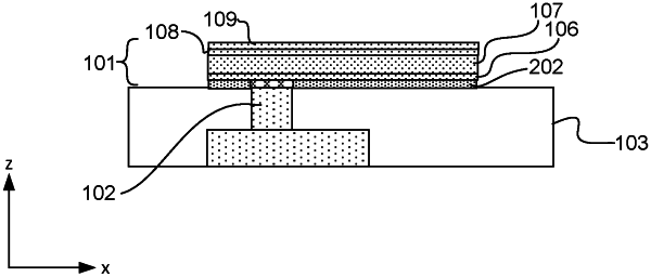
1. An integrated circuit (IC) package substrate, comprising:
a metal via extending to a top surface of a dielectric layer; and
a bond pad stack in contact with the metal via, the bond pad stack comprising a plurality of collocated layers, the collocated layers of the bond pad stack comprising:
a first layer comprising a reduced noble metal, a first portion of the reduced noble metal in contact with the metal via and a second portion of the reduced noble metal extending laterally from the metal via over the dielectric layer adjacent to the metal via, wherein a top of the metal via immediately adjacent the first portion of the reduced noble metal comprises oxidized metal; and
a second layer on the first layer, the second layer comprising a second metal.
|