| CPC H01L 23/49816 (2013.01) [H01L 21/4853 (2013.01); H01L 21/56 (2013.01); H01L 23/3121 (2013.01); H01L 23/49861 (2013.01); H01L 24/13 (2013.01); H01L 23/5385 (2013.01); H01L 2224/023 (2013.01); H01L 2225/107 (2013.01)] | 20 Claims |
|
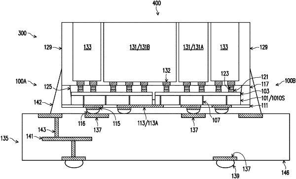
1. A semiconductor structure comprising:
a first interposer;
a second interposer laterally adjacent to the first interposer, wherein the second interposer is spaced apart from the first interposer;
a first molding material around the first interposer and around the second interposer;
a first die attached to a first side of the first interposer and attached to a first side of the second interposer, wherein the first side of the first interposer and the first side of the second interposer face the first die;
an underfill material between the first interposer and the first die and between the second interposer and the first die, wherein the first molding material surrounds the underfill material, wherein the first molding material and the underfill material have a coplanar surface; and
a second molding material around the first die, wherein the second molding material contacts the coplanar surface.
|