| CPC H01L 23/49503 (2013.01) [H01L 23/3107 (2013.01); H01L 23/49575 (2013.01); H01L 24/48 (2013.01); H01L 25/072 (2013.01); H01L 2224/48139 (2013.01); H01L 2224/48245 (2013.01)] | 20 Claims |
|
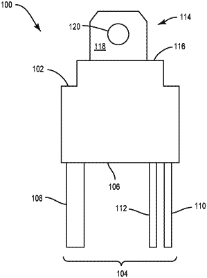
1. A semiconductor package, comprising:
a first die pad;
a first semiconductor die mounted on the first die pad;
an encapsulant body of electrically insulating material that encapsulates first die pad and the first semiconductor die;
a plurality of package leads that each protrude out of a first outer face of the encapsulant body;
a connection lug that protrudes out of a second outer face of the encapsulant body, the second outer face being opposite from the first outer face,
wherein the first semiconductor die comprises first and second voltage blocking terminals,
wherein the connection lug is electrically connected to one of the first and second voltage blocking terminals of the first semiconductor die, and
wherein a first one of the package leads is electrically connected to an opposite one of the first and second voltage blocking terminals of the first semiconductor die that the first connection lug is electrically connected to.
|