| CPC H01L 23/485 (2013.01) [H01L 21/4857 (2013.01); H01L 21/4867 (2013.01); H01L 21/568 (2013.01); H01L 21/6835 (2013.01); H01L 23/528 (2013.01); H01L 23/5226 (2013.01); H01L 23/5389 (2013.01); H01L 25/105 (2013.01); H01L 25/50 (2013.01); H01L 23/3128 (2013.01); H01L 23/49816 (2013.01); H01L 24/05 (2013.01); H01L 24/13 (2013.01); H01L 2221/68345 (2013.01); H01L 2221/68359 (2013.01); H01L 2224/022 (2013.01); H01L 2224/04105 (2013.01); H01L 2224/0508 (2013.01); H01L 2224/05624 (2013.01); H01L 2224/12105 (2013.01); H01L 2224/13147 (2013.01); H01L 2224/214 (2013.01); H01L 2224/32145 (2013.01); H01L 2224/32225 (2013.01); H01L 2224/48091 (2013.01); H01L 2224/48227 (2013.01); H01L 2224/73265 (2013.01); H01L 2224/73267 (2013.01); H01L 2224/92244 (2013.01); H01L 2224/97 (2013.01); H01L 2225/0651 (2013.01); H01L 2225/06568 (2013.01); H01L 2225/1035 (2013.01); H01L 2225/1041 (2013.01); H01L 2225/1058 (2013.01); H01L 2924/15311 (2013.01)] | 20 Claims |

|
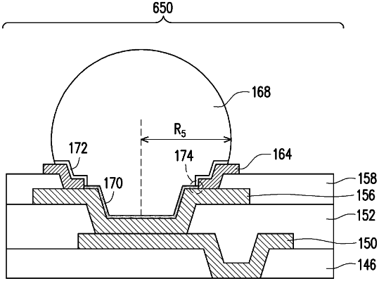
1. A device comprising:
an integrated circuit die;
a first dielectric layer over the integrated circuit die;
an under bump metallurgy extending through the first dielectric layer, the under bump metallurgy connected to the integrated circuit die;
a second dielectric layer over the under bump metallurgy and the first dielectric layer;
a conductive ring sealing an interface of the second dielectric layer and the under bump metallurgy, the conductive ring comprising a first conductive material;
a conductive connector extending through the conductive ring, the conductive connector connected to the under bump metallurgy, the first conductive material of the conductive ring extending between the conductive connector and the second dielectric layer;
a first intermetallic compound at an interface of the conductive connector and the under bump metallurgy; and
a second intermetallic compound at an interface of the conductive connector and the conductive ring, the first intermetallic compound and the second intermetallic compound being different compounds.
|