| CPC H01L 23/481 (2013.01) [H01L 21/565 (2013.01); H01L 23/5386 (2013.01); H01L 23/5389 (2013.01); H01L 24/16 (2013.01); H01L 25/0652 (2013.01); H01L 23/49811 (2013.01); H01L 23/49833 (2013.01); H01L 23/49838 (2013.01); H01L 23/5385 (2013.01); H01L 24/96 (2013.01); H01L 25/16 (2013.01); H01L 2224/16227 (2013.01); H01L 2224/16238 (2013.01); H01L 2924/182 (2013.01); H01L 2924/37001 (2013.01)] | 20 Claims |
|
1. A semiconductor device, comprising:
a large semiconductor die comprising conductive interconnects with a first encapsulant disposed around four side surfaces of the large semiconductor die, over an active surface of the large semiconductor die, and around the conductive interconnects;
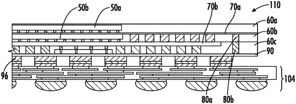
a first build-up interconnect structure disposed over the large semiconductor die and over the first encapsulant;
vertical conductive interconnects disposed over the first build-up interconnect structure and around an embedded device mount site;
an embedded device disposed over the embedded device mount site and completely within a footprint of the large semiconductor die, wherein the embedded device comprises through silicon vias (TSVs), and wherein the embedded device further comprises an active device, a semiconductor die comprising an active surface, an integrated passive device (IPD), or a passive device;
a single second encapsulant disposed over and contacting the first build-up interconnect structure, around the vertical conductive interconnects, and around and contacting at least five sides of the embedded device;
a second build-up interconnect structure disposed over the second encapsulant and configured to be electrically coupled to the TSVs of the embedded device and the vertical conductive interconnects; and
conductive bumps disposed over the second build-up interconnect structure and configured to couple the semiconductor device with other devices, wherein the conductive bumps comprise one or more of an input electrical contact, an output electrical contact, an i/o contact, a bump, a solder ball, a solder bump, a BGA, a LGA, land pads, copper pillars, and copper pillars with solder.
|