| CPC H01L 23/481 (2013.01) [H01L 25/0652 (2013.01); H01L 29/7827 (2013.01); H10B 41/27 (2023.02); H10B 43/27 (2023.02); H01L 2225/06541 (2013.01)] | 20 Claims |
|
1. A semiconductor device, comprising:
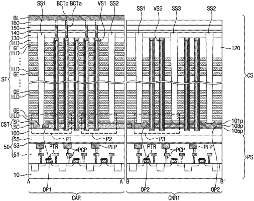
a substrate including a cell array region and a connection region;
a stack including electrodes vertically stacked on the substrate;
a source conductive pattern on the cell array region and between the substrate and the stack;
a dummy insulating pattern on the connection region and between the substrate and the stack;
a conductive support pattern between the stack and the source conductive pattern and between the stack and the dummy insulating pattern;
a plurality of first vertical structures on the cell array region and penetrating the stack, the conductive support pattern, and the source conductive pattern
a first separation structure penetrating the stack and extending in a first direction,
wherein the first separation structure includes a first portion on the cell array region and a second portion on the connection region, and
wherein the second portion of the first separation structure is in contact with a top surface of the conductive support pattern and is vertically spaced apart from the dummy insulating pattern.
|