| CPC H01L 23/481 (2013.01) [H01L 23/49816 (2013.01); H01L 23/49838 (2013.01); H01L 23/5226 (2013.01); H01L 23/5283 (2013.01); H01L 23/5286 (2013.01); H01L 23/5384 (2013.01); H01L 23/5386 (2013.01); H01L 23/53209 (2013.01); H01L 24/08 (2013.01); H01L 24/16 (2013.01); H01L 25/0652 (2013.01); H01L 25/0657 (2013.01); H01L 2224/08146 (2013.01); H01L 2224/08147 (2013.01); H01L 2224/16146 (2013.01); H01L 2224/16147 (2013.01); H01L 2224/16227 (2013.01); H01L 2224/16237 (2013.01); H01L 2225/06513 (2013.01); H01L 2225/06517 (2013.01); H01L 2225/06544 (2013.01); H01L 2225/06548 (2013.01); H01L 2924/1431 (2013.01); H01L 2924/1434 (2013.01)] | 20 Claims |
|
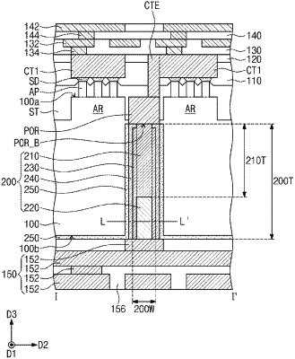
1. A semiconductor device, comprising:
a semiconductor substrate having a first surface and a second surface, which are opposite to each other;
an active pattern protruding from the first surface of the semiconductor substrate, the active pattern including a source/drain region;
a power rail electrically connected to the source/drain region;
a power delivery network disposed on the second surface of the semiconductor substrate;
a device isolation layer disposed on the first surface of the semiconductor substrate and covering a side surface of the active pattern,
wherein the power rail is buried in the device isolation layer; and
a penetration via structure penetrating the semiconductor substrate and electrically connected to the power rail and the power delivery network,
wherein the penetration via structure comprises:
a first conductive pattern electrically connected to the power rail; and
a second conductive pattern electrically connected to the power delivery network,
wherein the first conductive pattern comprises a material different from the second conductive pattern.
|