| CPC H01L 23/3107 (2013.01) [H01L 21/56 (2013.01); H01L 23/5286 (2013.01); H01L 24/11 (2013.01); H01L 24/14 (2013.01); H01L 24/43 (2013.01); H01L 24/45 (2013.01)] | 9 Claims |

|
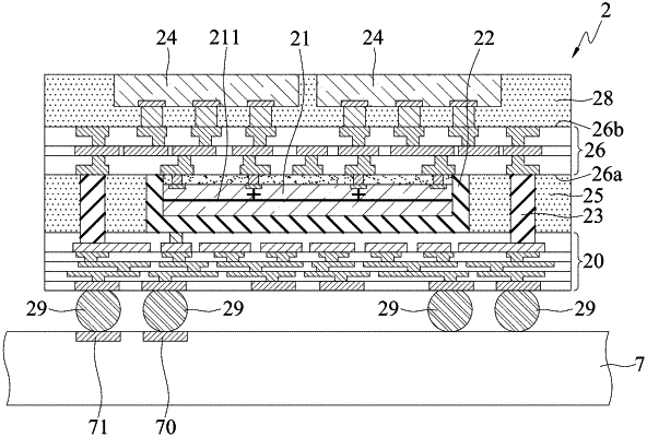
1. An electronic package, comprising:
an encapsulant;
a first electronic component embedded in the encapsulant, wherein the first electronic component includes an active surface and a non-active surface opposite to the active surface and side surfaces adjacent to the active surface and the non-active surface, wherein at least one electrode pad is disposed on the active surface, and at least one wire electrically connected with the at least one electrode pad is provided inside the first electronic component; and
at least one conductive layer formed on the first electronic component and embedded in the encapsulant and electrically connected with the at least one wire, wherein the at least one conductive layer is free from being formed on the at least one electrode pad.
|