| CPC H01L 23/13 (2013.01) [H01L 21/4853 (2013.01); H01L 25/105 (2013.01); H01L 25/50 (2013.01); H01L 2225/1023 (2013.01); H01L 2225/1058 (2013.01)] | 20 Claims |

|
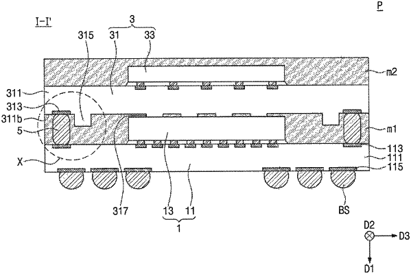
1. A semiconductor package, comprising:
a lower package;
an upper substrate on the lower package; and
a plurality of connection members electrically connecting the lower package to the upper substrate,
wherein the lower package comprises:
a lower substrate; and
a lower semiconductor chip on the lower substrate,
wherein the upper substrate comprises;
an upper substrate body;
upper connection pads provided on the upper substrate body and combined with the plurality of connection members, respectively; and
auxiliary members extending from a bottom surface of the upper substrate body toward the lower substrate, wherein the auxiliary members comprise the same insulating material as the upper substrate body,
wherein the plurality of connection members are arranged in a first horizontal direction to form a first connection member column,
wherein the auxiliary members are arranged in the first horizontal direction to form a first auxiliary member column,
wherein the first connection member column and the first auxiliary member column are located between a side surface of the lower semiconductor chip and a side surface of the lower substrate,
the first auxiliary member column is spaced apart from the first connection member column, in a second horizontal direction crossing the first horizontal direction,
wherein, the semiconductor package further comprises a lower mold layer provided on the lower substrate, wherein a side surface of the auxiliary member contacts the lower mold layer.
|