| CPC H01L 21/823462 (2013.01) [G11C 5/063 (2013.01); H01L 21/8221 (2013.01); H01L 21/8232 (2013.01); H01L 21/823487 (2013.01); H01L 23/5226 (2013.01); H10B 41/27 (2023.02); H10B 41/35 (2023.02); H10B 43/27 (2023.02); H10B 43/30 (2023.02); H10B 43/35 (2023.02)] | 20 Claims |
|
1. A method of manufacturing an integrated circuit device, the method comprising:
forming, on a substrate, a structure comprising a plurality of first films and a plurality of second films alternately stacked with the plurality of first films;
forming a channel hole that extends through the structure;
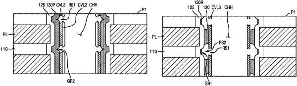
forming, in the channel hole, a plurality of indented spaces by removing portions of the plurality of first films through the channel hole;
forming, in the channel hole, a blocking dielectric film comprising a plurality of first grooves that are on the plurality of indented spaces, respectively, a preliminary charge storage film comprising a plurality of second grooves that are on the plurality of first grooves, respectively, and a first cover sacrificial layer comprising a plurality of third grooves that are on the plurality of second grooves, respectively, a plurality of first cover layers in the plurality of third grooves, respectively, and a second cover layer on the first cover sacrificial layer;
exposing portions of the first cover sacrificial layer by removing the plurality of first cover layers;
forming a third cover layer comprising a first recess space that exposes one of the plurality of second grooves by removing one of the portions of the first cover sacrificial layer; and
forming at least one charge storage film by removing a portion of the preliminary charge storage film through the first recess space.
|