| CPC H01L 21/76897 (2013.01) [H01L 21/0217 (2013.01); H01L 21/02126 (2013.01); H01L 21/02211 (2013.01); H01L 21/02227 (2013.01); H01L 21/02271 (2013.01); H01L 21/02301 (2013.01); H01L 21/02312 (2013.01); H01L 21/0337 (2013.01); H01L 21/28247 (2013.01); H01L 21/28525 (2013.01); H01L 21/28568 (2013.01); H01L 21/3105 (2013.01); H01L 21/31116 (2013.01); H01L 21/31144 (2013.01); H01L 21/76802 (2013.01); H01L 21/76826 (2013.01); H01L 21/76829 (2013.01); H01L 21/823821 (2013.01); H01L 23/5226 (2013.01); H01L 29/66545 (2013.01); H01L 29/66795 (2013.01); H01L 29/785 (2013.01); H01L 21/32 (2013.01); H01L 21/32134 (2013.01); H01L 21/32135 (2013.01); H01L 29/7848 (2013.01)] | 20 Claims |
|
1. A method comprising:
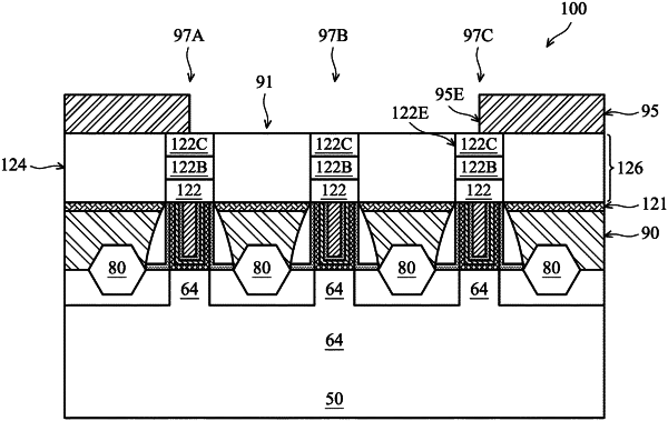
forming a gate structure over a substrate, wherein the gate structure is surrounded by a first dielectric layer;
forming a mask structure over the gate structure and over the first dielectric layer, wherein the mask structure comprises a dielectric structure over the gate structure and over gate spacers of the gate structure, and a second dielectric layer over the first dielectric layer around the dielectric structure;
forming a patterned dielectric layer over the mask structure, the patterned dielectric layer exposing a portion of the second dielectric layer and a portion of the dielectric structure;
removing the exposed portion of the second dielectric layer and a portion of the first dielectric layer underlying the exposed portion of the second dielectric layer, thereby forming a recess exposing a source/drain region adjacent to the gate structure; and
filling the recess with a conductive material.
|