| CPC H01L 21/76856 (2013.01) [H01L 21/76843 (2013.01); H01L 21/76874 (2013.01); H01L 21/7684 (2013.01)] | 17 Claims |
|
1. A method for copper plating filling, comprising a plurality of steps:
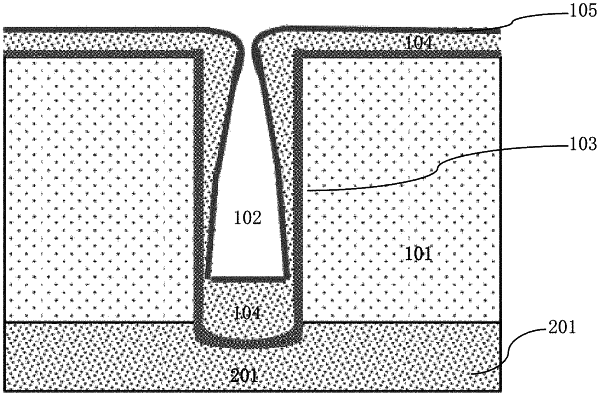
before performing step 1, providing a semiconductor substrate, comprising a series of interconnection structures each comprising a metal wire layer and a dielectric layer;
step 1: forming a hole in the dielectric layer;
step 2: forming a copper diffusion barrier layer on an inner surface of the hole, and forming a copper seed layer on a surface of the copper diffusion barrier layer, wherein the copper diffusion barrier layer and the copper seed layer are also disposed extending to a top surface of the dielectric layer outside the hole;
step 3: allowing a waiting time to grow a protective copper oxide layer on a surface of the copper seed layer, and increasing the waiting time between after forming the copper seed layer and before transferring the semiconductor substrate into a plating machine to perform a copper plating process so as to widen a window of growing the protective copper oxide layer;
step 4: performing a reduction process by applying a solution on the protective copper oxide layer following oxidation of the copper seed layer surface during the time of waiting time; and
step 5: filling a copper plating layer on the surface of the copper seed surface into the hole and over the dielectric layer outside the hole in the copper plating process afterwards and connecting the copper filled hole in the dielectric layer to the metal wire layer;
wherein, the protective copper oxide layer on the surface of the copper seed layer is reduced to copper in the reduction process, and wherein a thickness of the copper seed layer on the inner surface of the hole is kept uniform.
|