| CPC H01L 21/76816 (2013.01) [H01L 21/0335 (2013.01); H01L 21/0337 (2013.01); H01L 21/0338 (2013.01); H01L 21/76877 (2013.01)] | 20 Claims |
|
1. A method comprising:
forming an interconnect dielectric layer arranged over a substrate;
depositing multiple hard mask layers over the interconnect dielectric layer;
depositing a first patterning layer over the multiple hard mask layers;
forming a first masking structure over the first patterning layer, wherein openings in the first masking structure are formed by way of a first extreme ultraviolet (EUV) lithography process;
removing portions of the first patterning layer according to the first masking structure to pattern the first patterning layer;
forming a second masking structure within the patterned first patterning layer;
patterning a topmost one of the hard mask layers according to the second masking structure;
forming a third masking structure over the topmost one of the hard mask layers, wherein openings in the third masking structure are formed by way of a second EUV lithography process;
performing removal processes to pattern the multiple hard mask layers and form openings in the interconnect dielectric layer; and
forming interconnect wires within the openings of the interconnect dielectric layer,
wherein a first interconnect wire extends from an upper surface of the interconnect dielectric layer and towards the substrate in a first direction to contact an interconnect via,
wherein first outermost sidewalls of the first interconnect wire are parallel to one another and normal to a second direction perpendicular to the first direction,
wherein second outermost sidewalls of the first interconnect wire are parallel to one another and normal to a third direction perpendicular to the first and second directions, and
wherein rounded corners couple the first outermost sidewalls to the second outermost sidewalls.
|
|
8. A method comprising:
forming an interconnect dielectric layer arranged over a substrate;
depositing multiple hard mask layers over the interconnect dielectric layer;
depositing a first patterning layer over the multiple hard mask layers;
forming a first masking structure over the first patterning layer by way of a first extreme ultraviolet (EUV) lithography process;
removing portions of the first patterning layer according to the first masking structure to pattern the first patterning layer;
forming a second masking structure within the patterned first patterning layer;
patterning a topmost one of the hard mask layers according to the second masking structure;
forming a second patterning layer over the topmost one of the hard mask layers;
forming a third masking structure over the second patterning layer by way of a second EUV lithography process;
removing portions of the second patterning layer and the multiple hard mask layers according to the third masking structure and the topmost one of the hard mask layers to form openings in the interconnect dielectric layer; and
forming interconnect wires within the openings of the interconnect dielectric layer,
wherein a first interconnect wire and a second interconnect wire extend through the interconnect dielectric layer in a first direction,
wherein first outermost sidewalls of the first interconnect wire are spaced apart from one another by a first distance in a second direction perpendicular to the first direction,
wherein second outermost sidewalls of the first interconnect wire are spaced apart from one another by a second distance in a third direction perpendicular to the first and second directions,
wherein the first distance is greater than the second distance, and
wherein the first interconnect wire is spaced apart from the second interconnect wire in the second direction by a third distance that is less than or equal to the second distance.
|
|
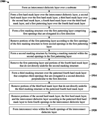
14. A method comprising:
forming an interconnect dielectric layer over a substrate;
forming a first hard mask layer over the interconnect dielectric layer, a second hard mask layer over the first hard mask layer, a third hard mask layer over the second hard mask layer, a fourth hard mask layer over the third hard mask layer, and a first patterning layer over the fourth hard mask layer;
forming a first masking structure over the first patterning layer comprising first openings that are elongated in a first direction;
removing portions of the first patterning layer according to the first openings of the first masking structure to form second openings in the first patterning layer;
forming a second masking structure by forming a masking material within the second openings in the first patterning layer;
removing the first patterning layer and portions of the fourth hard mask layer that do not directly underlie the second masking structure to pattern the fourth hard mask layer;
forming a third masking structure over the patterned fourth hard mask layer that comprises third openings that are elongated in a second direction perpendicular to the first direction;
removing portions of the third hard mask layer that do not directly underlie the third masking structure or the patterned fourth hard mask layer to pattern the third hard mask layer;
removing portions of the second hard mask layer, the first hard mask layer, and the interconnect dielectric layer according to the patterned third hard mask layer to form fourth openings in the interconnect dielectric layer; and
forming interconnect wires within the fourth openings of the interconnect dielectric layer.
|