| CPC H01L 21/764 (2013.01) [H01L 29/0653 (2013.01); H01L 29/0847 (2013.01); H01L 29/161 (2013.01); H01L 29/165 (2013.01); H01L 29/1608 (2013.01); H01L 29/24 (2013.01); H01L 29/66795 (2013.01); H01L 29/7848 (2013.01); H01L 29/7851 (2013.01); H01L 29/7853 (2013.01)] | 20 Claims |
|
1. A semiconductor device comprising:
a raised portion of a substrate, the raised portion of the substrate having a first top surface higher than a second top surface of the substrate;
a first fin extending from the raised portion of the substrate, the first fin comprising a first semiconductor material;
a second fin extending from the raised portion of the substrate, the second fin being adjacent the first fin, the second fin comprising the first semiconductor material;
a first semiconductor layer on the first fin and a second semiconductor layer on the second fin, the first semiconductor layer and the second semiconductor layer having a first dopant concentration;
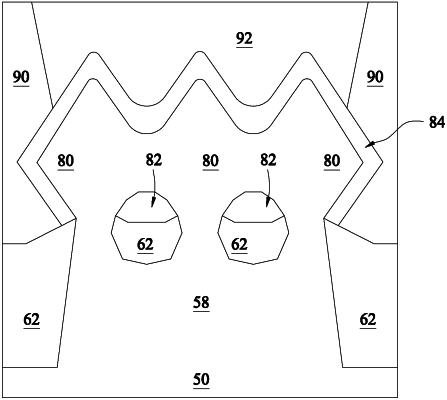
a first isolation region on the first top surface of the raised portion of the substrate and between the first fin and the second fin;
a second isolation region along opposing sidewalls of the raised portion of the substrate;
a first epitaxial region over the first fin, the first epitaxial region comprising a second semiconductor material;
a second epitaxial region over the second fin, the second epitaxial region comprising the second semiconductor material, wherein the first epitaxial region is merged with the second epitaxial region, wherein the first epitaxial region is on the first semiconductor layer and the second epitaxial region is on the second semiconductor layer, the first epitaxial region and the second epitaxial region having a second dopant concentration greater than the first dopant concentration;
a capping layer directly on the first epitaxial region and the second epitaxial region, wherein the capping layer has a third dopant concentration less than the second dopant concentration;
a first dielectric layer on the first isolation region, the first dielectric layer extending from the first epitaxial region to the second epitaxial region, wherein the first epitaxial region and the second epitaxial region extends over the first dielectric layer, wherein a surface of the first epitaxial region and a surface of the second epitaxial region facing the first dielectric layer is free of the first dielectric layer;
a gate structure along sidewalls and over upper surfaces of the first fin and the second fin;
a source/drain region in the first epitaxial region and the second epitaxial region; and
a void interposed between the source/drain region and the first isolation region, the first dielectric layer being interposed between the void and the first isolation region.
|