| CPC H01L 21/76275 (2013.01) [H01L 21/76254 (2013.01)] | 20 Claims |
|
1. A method for fabricating a strained semiconductor-on-insulator substrate, the method comprising:
epitaxially growing an intermediate layer on a carrier substrate, and epitaxially growing a monocrystalline semiconductor layer on the intermediate layer, the carrier substrate, the intermediate layer, and the carrier substrate forming at least a portion of a donor substrate;
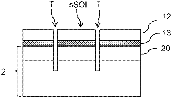
providing a receiving substrate comprising a strained monocrystalline semiconductor material on a base substrate;
bonding the donor substrate and the receiving substrate together to form a bonded structure;
selectively etching the carrier substrate with respect to the intermediate layer to remove the carrier substrate from the bonded structure;
selectively etching the intermediate layer with respect to the monocrystalline semiconductor layer to remove the intermediate layer from the bonded structure and expose a surface of the monocrystalline semiconductor layer, the exposed surface having a surface roughness of 3 Å RMS or less as measured by atomic force microscopy over a scan of 30×30 μm2; and
imparting strain on the monocrystalline semiconductor layer using the strained monocrystalline semiconductor material.
|