| CPC H01L 21/681 (2013.01) [H01L 21/67092 (2013.01); H01L 21/6838 (2013.01)] | 19 Claims |
|
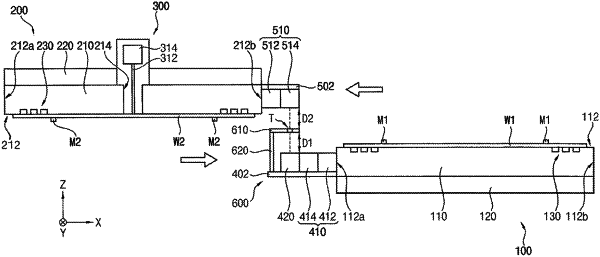
1. A wafer bonding apparatus, comprising:
a first stage having a first surface, the first stage being configured to hold a first wafer on the first surface;
a second stage having a second surface, the second stage being configured to hold a second wafer on the second surface, the first surface and the second surface facing each other;
a first target image sensor on an outer portion of the first stage;
a second target image sensor on an outer portion of the second stage;
a target portion on the first stage or the second stage, the target portion having a target plate fixedly installed and spaced apart from the first target image sensor or the second target image sensor by a predetermined distance;
a controller connected to the first target image sensor and the second target image sensor,
wherein, in an alignment measurement of the first stage and the second stage, the first stage and the second stage are movable so that the first target image sensor and the second target image sensor face each other and the target plate is between the first target image sensor and the second target image sensor facing each other, and
wherein the controller is configured to control operations of the first stage and the second stage based on results of the alignment measurement of the first stage and the second stage.
|