| CPC H01L 21/67294 (2013.01) [H01L 21/67276 (2013.01)] | 20 Claims |
|
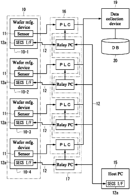
1. A wafer manufacturing system comprising:
a wafer manufacturing device provided with a sensor;
a host PC that is connected to the wafer manufacturing device via a data communication line and controls the wafer manufacturing device;
a logic controller that is external and independent from the wafer manufacturing device, wherein the logic controller samples and stores an analog output signal of the sensor; and
a relay PC that is separate from the wafer manufacturing device and extracts tracking information transmitted on the data communication line for a wafer or a single crystal that is being processed by the wafer manufacturing device and sends the tracking information to the logic controller, wherein
an analog output signal of the sensor is split into two branches where one analog output signal is used to control operations of the wafer manufacturing device and the other analog output signal is sent to the logic controller for collecting data, wherein
the logic controller stores a digital value of the other analog output signal of the sensor in association with the tracking information that is sent from the relay PC, and wherein
the relay PC receives and sends signals between the host PC and the wafer manufacturing device.
|