| CPC H01L 21/28556 (2013.01) [H01L 21/28568 (2013.01); H01L 21/76805 (2013.01); H01L 21/76832 (2013.01); H01L 21/76895 (2013.01); H01L 23/535 (2013.01); H01L 23/53257 (2013.01); H01L 23/53295 (2013.01); H01L 29/0847 (2013.01); H01L 29/41791 (2013.01); H01L 29/66545 (2013.01); H01L 29/66795 (2013.01); H01L 29/785 (2013.01); H01L 29/7851 (2013.01); C23C 16/16 (2013.01)] | 20 Claims |

|
1. A semiconductor device, comprising:
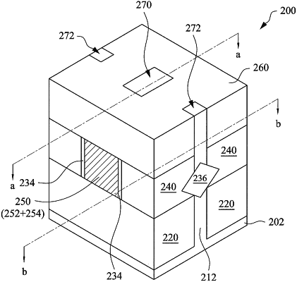
a fin structure having a first portion extending through a first region comprising a gate feature and a second portion extending through a second region comprising a pair of source/drain features, wherein the first portion of the fin structure has a first height and the second portion of the fin structure has a second height, wherein the first height is greater than the second height; and
a gate electrode, of the gate feature, located in a first dielectric layer located above an oxide layer, wherein the first portion of the fin structure vertically extends into the gate electrode, wherein the pair of source/drain features are disposed at respective sides of the gate feature and at least partially located in the oxide layer and at least partially located in the first dielectric layer, wherein bottom surfaces of the pair of source/drain features directly contact respective portions of a top surface of the second portion of the fin structure;
a first contact structure extending through a second dielectric layer located above the first dielectric layer and directly contacting a top surface of the gate electrode of the gate feature; and
a second contact structure extending through the second dielectric layer and at least partially through the first dielectric layer to directly contact a source feature of the pair of source/drain features.
|