| CPC H01L 21/0335 (2013.01) [H01J 37/3244 (2013.01); H01L 21/02315 (2013.01); H01L 21/31144 (2013.01); H01J 2237/3321 (2013.01)] | 22 Claims |
|
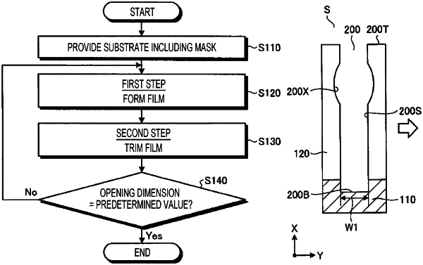
1. A method of processing a substrate including an etching target film and a mask having an opening formed on the etching target film, comprising:
(a) providing the substrate on a stage in a chamber;
(b) forming a film having a thickness that differs along a film thickness direction of the mask, on a side wall of the opening; and
(c) trimming the film,
wherein when (b) is repeatedly performed n or more times (n is a natural number of 2 or more), a position and a thickness of the film formed in (b) are changed by changing a processing condition in an n-th processing and an (n−1)-th processing, and
a variation in an opening dimension of the opening in the film thickness direction of the mask after (c) is smaller than a variation in an opening dimension of the opening in the film thickness direction of the mask before (c).
|