US 11,728,164 B2
Selective PEALD of oxide on dielectric
Eva Tois, Helsinki (FI); Viljami Pore, Helsinki (FI); Suvi Haukka, Helsinki (FI); Toshiya Suzuki, Tokyo (JP); Lingyun Jia, Helsinki (FI); Sun Ja Kim, Helsinki (FI); and Oreste Madia, Leuven (BE)
Assigned to ASM IP HOLDING B.V., Almere (NL)
Filed by ASM IP HOLDING B.V., Almere (NL)
Filed on Oct. 11, 2021, as Appl. No. 17/450,538.
Application 17/450,538 is a continuation of application No. 16/605,475, granted, now 11,170,993, previously published as PCT/US2018/030979, filed on May 3, 2018.
Claims priority of provisional application 62/507,078, filed on May 16, 2017.
Prior Publication US 2022/0076949 A1, Mar. 10, 2022
This patent is subject to a terminal disclaimer.
Int. Cl. C23C 16/40 (2006.01); C23C 16/455 (2006.01); H01L 21/02 (2006.01)
CPC H01L 21/02274 (2013.01) [C23C 16/401 (2013.01); C23C 16/45542 (2013.01); C23C 16/45553 (2013.01); H01L 21/0228 (2013.01); H01L 21/02126 (2013.01); H01L 21/02164 (2013.01); H01L 21/02186 (2013.01); H01L 21/02216 (2013.01)] 20 Claims
OG exemplary drawing
 
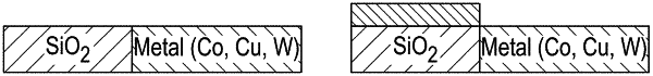
1. A plasma enhanced atomic layer deposition (PEALD) process for selectively depositing an oxide on a dielectric surface of a substrate relative to a TiN surface comprising:
providing a substrate comprising a dielectric surface and a TiN surface;
conducting at least one deposition cycle comprising alternately and sequentially contacting the substrate with a first silicon precursor comprising oxygen and a second reactant comprising reactive species from a plasma generated in a gas comprising hydrogen and not oxygen.