| CPC H01L 21/02266 (2013.01) [C23C 14/08 (2013.01); C23C 14/34 (2013.01); H01L 21/02172 (2013.01); H01L 21/02293 (2013.01)] | 14 Claims |
|
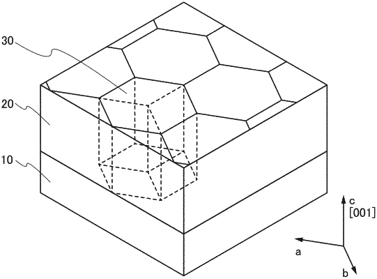
1. A method for manufacturing a metal oxynitride film,
wherein the metal oxynitride film is epitaxially grown in contact with a single crystal substrate by a sputtering method using an oxide target with a gas containing a nitrogen gas introduced,
wherein the oxide target comprises zinc,
wherein the single crystal substrate during deposition of the metal oxynitride film has a temperature that is higher than or equal to 80° C. and lower than or equal to 400° C., and
wherein a flow rate of the nitrogen gas is greater than or equal to 50% and lower than or equal to 100% of a total flow rate of the gas.
|