US 11,728,160 B2
Method of forming oxide film including two non-oxygen elements, method of manufacturing semiconductor device, method of forming dielectric film, and semiconductor device
Younsoo Kim, Yongin-si (KR); Haeryong Kim, Seongnam-si (KR); Seungmin Ryu, Hwaseong-si (KR); Sunmin Moon, Yongin-si (KR); Jeonggyu Song, Seongnam-si (KR); Changsu Woo, Seoul (KR); Kyooho Jung, Seoul (KR); and Younjoung Cho, Hwaseong-si (KR)
Assigned to Samsung Electronics Co., Ltd., Gyeonggi-do (KR)
Filed by Samsung Electronics Co., Ltd., Suwon-si (KR)
Filed on Jul. 15, 2021, as Appl. No. 17/376,403.
Application 17/376,403 is a continuation of application No. 16/791,189, filed on Feb. 14, 2020, granted, now 11,081,338.
Claims priority of application No. 10-2019-0091159 (KR), filed on Jul. 26, 2019.
Prior Publication US 2021/0343524 A1, Nov. 4, 2021
This patent is subject to a terminal disclaimer.
Int. Cl. H01L 21/02 (2006.01)
CPC H01L 21/02164 (2013.01) [H01L 21/0228 (2013.01)] 20 Claims
OG exemplary drawing
 
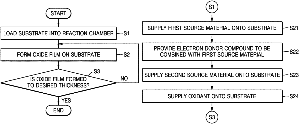
1. A method of forming an oxide film including two non-oxygen elements, the method comprising:
providing an electron donor compound on a substrate;
providing a first source material on the substrate, the first source material comprising a first central element; and
providing an oxidant on the substrate to form an oxide film,
wherein the electron donor includes an unshared electron pair or includes a double bond or a triple bond.