| CPC H01L 21/02074 (2013.01) [H01L 21/7684 (2013.01); H01L 21/76898 (2013.01); H01L 23/481 (2013.01); H01L 23/522 (2013.01)] | 4 Claims |
|
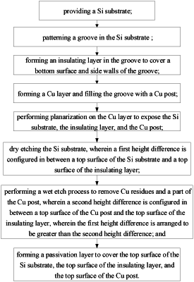
1. A method for preparing a semiconductor structure, comprising following steps of:
providing a Si substrate;
patterning a groove in the Si substrate;
forming an insulating layer in the groove to cover a bottom surface and side walls of the groove;
forming a Cu layer and filling the groove with a Cu post;
performing planarization on the Cu layer to expose the Si substrate, the insulating layer, and the Cu post;
dry etching the Si substrate, wherein a first height difference is configured in between a top surface of the Si substrate and a top surface of the insulating layer;
performing a wet etch process to remove Cu residues and a part of the Cu post, wherein a second height difference is configured in between a top surface of the Cu post and the top surface of the insulating layer, wherein the first height difference is arranged to be greater than the second height difference, wherein the first height difference is in a range of 2 μm to 5 μm and the second height difference is in a range of 0.1 μm to 0.5 μm; and
forming a passivation layer to cover the top surface of the Si substrate, the top surface of the insulating layer, and the top surface of the Cu post.
|