| CPC H01G 4/30 (2013.01) [H01G 4/008 (2013.01); H01G 4/012 (2013.01); H01G 4/1209 (2013.01); H01G 4/224 (2013.01)] | 14 Claims |
|
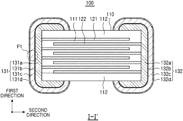
1. A multilayer electronic component comprising:
a body including dielectric layers and internal electrodes alternately disposed with the dielectric layers; and
an external electrode disposed on the body,
wherein the external electrode includes:
an electrode layer connected to the internal electrode;
an Sn plating layer disposed on the electrode layer;
an Ni plating layer disposed on the Sn plating layer; and
a plating layer including Pd disposed on the Ni plating layer, and
wherein a thickness of the Sn plating layer from the electrode layer to the Ni plating layer is 0.02 to 0.1 μm.
|