| CPC H01F 27/36 (2013.01) [H01F 27/2804 (2013.01); H01F 27/323 (2013.01); H01G 4/012 (2013.01); H01G 4/30 (2013.01); H01F 2027/2809 (2013.01)] | 20 Claims |
|
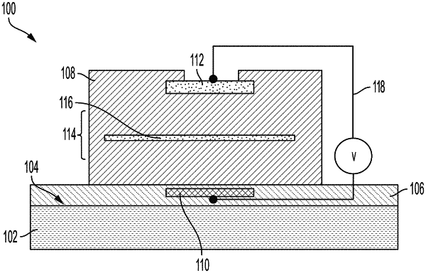
1. An isolated micro-scale passive device configured to be disposed on a substrate comprising an upper surface, the isolated micro-scale passive device comprising:
a first planar conductor;
a second planar conductor configured to be disposed between the first planar conductor and the substrate;
an insulator layer disposed between the first planar conductor and the second planar conductor; and
a floating conductive layer in the insulator layer, wherein:
the first planar conductor has a first spacing from the floating conductive layer;
the second planar conductor has a second spacing from the floating conductive layer;
the first spacing is less than the second spacing such that the first spacing and the second spacing are configured to substantially balance a first capacitance of the isolated micro-scale passive device with a second capacitance of the isolated micro-scale passive device;
the first capacitance comprises:
a capacitance between the floating conductive layer and the second planar conductor; and
a capacitance between the floating conductive layer and the substrate; and
the second capacitance comprises a capacitance between the floating conductive layer and the first planar conductor.
|