| CPC G11C 13/0069 (2013.01) [G11C 11/5678 (2013.01); G11C 13/0004 (2013.01); G11C 13/0033 (2013.01); H10B 63/80 (2023.02); H10N 70/231 (2023.02); H10N 70/882 (2023.02); G11C 2013/0092 (2013.01)] | 13 Claims |
|
1. A resistive memory device comprising:
a memory cell array including a plurality of memory cells, a memory cell comprising a memory element programmable to a plurality of resistance states;
a write circuit configured to program the memory cell to a target resistance state; and
a control circuitry configured to control a write pulse and a post-write pulse to be applied to the memory cell, wherein
the post-write pulse follows the write pulse,
the memory cell is programmed to the target resistance state in response to the write pulse, and
a resistance of the memory cell that is in the target resistance state is increased in response to the post-write pulse,
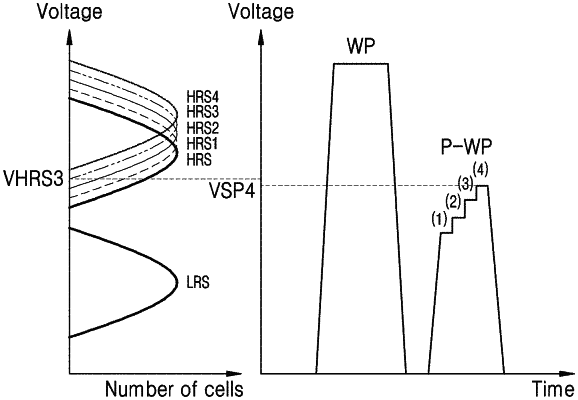
wherein the post-write pulse is a single pulse having at least n stepped-up voltage levels, n being an integer equal to or more than 2, each of the at least n stepped-up voltage levels having a time period smaller than the write pulse, and
wherein the at least n stepped-up voltage levels have different time periods;
wherein the target resistance state is a resistive state having a relatively high resistance level among 2m resistance states to which the memory cell is programmed, m being a natural number,
wherein the control circuitry is further configured to
control each of the at least n stepped-up voltage levels to increase with a certain amplitude, and
control an n-th stepped-up voltage level of the at least n stepped-up voltage levels of the post-write pulse to be applied to the memory cell such that the n-th stepped-up voltage level is lower than a minimum threshold voltage level of the target resistance state that is changed by an (n−1)-th stepped-up voltage level of the post-write pulse.
|