| CPC G11C 7/1039 (2013.01) [G11C 7/109 (2013.01); G11C 7/1048 (2013.01); G11C 7/1063 (2013.01); G11C 7/1066 (2013.01); G11C 7/1093 (2013.01); G11C 8/08 (2013.01)] | 17 Claims |

|
1. A nonvolatile memory device comprising:
a memory cell array including a plurality of nonvolatile memory cells; and
a row decoder connected with the memory cell array through wordlines, wherein the row decoder is configured to,
precharge a first wordline corresponding to a first row address from among the wordlines in response to receiving the first row address together with a first command, and
maintain a precharge state of the first wordline in response to receiving a second row address identical to the first row address together with a second command following the first command, and
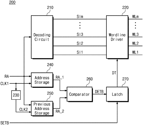
wherein the row decoder includes,
a first circuit configured to output row address signals, which are input to the first circuit through row address input lines and correspond to the first row address or the second row address, as first internal address signals,
a second circuit configured to delay the row address signals transferred through the row address input lines to output second internal address signals, and
a third circuit configured to output an output signal based on the first internal address signal and the second internal address signals.
|