| CPC G09G 3/3648 (2013.01) [G02F 1/1345 (2013.01); G02F 1/13452 (2013.01); G02F 1/136286 (2013.01); G09G 2310/0202 (2013.01)] | 12 Claims |
|
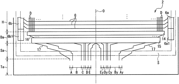
1. An active matrix substrate comprising:
data lines and scanning lines that are provided in a display region of the active matrix substrate, the data lines and the scanning lines being arranged in a matrix;
switching elements connected to each of the data lines and the scanning lines;
terminals that are provided at a peripheral region of the active matrix substrate to input external signals to the data lines; and
signal lines that are in a line region between the display region and the peripheral region; wherein
one end of each of the signal lines is electrically connected to at least one of the data lines, and another end of each of the signal lines is electrically connected to one of the terminals;
each of the signal lines includes a first line portion provided on a display region side of the signal lines, a second line portion provided on a peripheral region side of the signal lines, and a connection portion that connects the first line portion and the second line portion;
the first line portion and the second line portion of one of the signal lines include a first conductive layer and a second conductive layer, respectively, the first conductive layer and the second conductive layer being different from each other, and the first line portion and the second line portion of another one of the signal lines which is adjacent to the one of the signal lines include the second conductive layer and the first conductive layer, respectively;
the signal lines are divided into a first signal line group and a second signal line group that is close to the first signal line group;
the first line portions of the first signal line group extend in a first direction, and the first line portions of the second signal line group extend in a second direction that is different from the first direction.
|