| CPC G09G 3/3291 (2013.01) [G09G 2310/027 (2013.01)] | 16 Claims |
|
1. A display driving circuit configured to drive a display panel, the display panel comprising a plurality of data lines, a plurality of sensing lines, a plurality of gate lines, and a plurality of sub-pixels connected to the plurality of data lines, the plurality of gate lines and the plurality of sensing lines, wherein each row of the plurality of sub-pixels comprising at least two gate lines, the display driving circuit comprising:
a data driver integrated circuit configured to drive the plurality of data lines, wherein the data driver integrated circuit comprises:
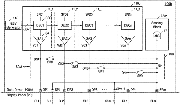
a plurality of digital-analog converters (DACs) each configured to perform digital-analog conversion with respect to received sub-pixel data to generate output voltages and provide the output voltages to the plurality of data lines;
a sensing block configured to measure analog grayscale voltages output from the plurality of DACs in a calibration period and measure pixel voltages of the plurality of sub-pixels received from the plurality of sensing lines in a sensing period, and
a plurality of switches connected to the plurality of DACs and to the sensing block,
wherein each of the plurality of DACs is connected to the sensing block by one of the plurality of switches, and
wherein:
in a data driving period, a pulse of a gate-on voltage is selectively applied to a first gate line of a first row of the plurality of sub-pixels, and a calibration mode signal is configured to turn off the plurality of switches to electrically disconnect the plurality of DACs from the sensing block and the plurality of DACs provide the output voltages to the plurality of sub-pixels,
in the sensing period, a pulse of a gate-on voltage is selectively applied to a second gate line of the first row of the plurality of sub-pixels to turn on the plurality of sensing lines of the first row of the plurality of sub-pixels, and the calibration mode signal is configured to turn off the plurality of switches to electrically disconnect the plurality of DACs from the sensing block and the sensing block senses the pixel voltages from the plurality of sensing lines, and
in the calibration period, a gate-off voltage is applied to all of the first gate line and the second gate line of the plurality of sub-pixels, and the calibration mode signal is configured to turn on the plurality of switches to electrically connect the plurality of DACs to the sensing block such that the analog grayscale voltages output from the plurality of DACs are directly provided to the sensing block internally in the data driver integrated circuit and the sensing block measures the analog grayscale voltages output from the plurality of DACs.
|