| CPC G09G 3/3266 (2013.01) [G09G 3/3233 (2013.01); G09G 2300/0819 (2013.01); G09G 2300/0842 (2013.01); G09G 2310/08 (2013.01)] | 20 Claims |
|
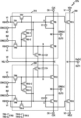
1. A scan driver comprising a plurality of stages, each of the plurality of stages comprising:
a first controller configured to control voltage levels of a first control node and a second control node in response to a first start signal and a second start signal, and to output a first carry signal;
a second controller configured to control voltage levels of a third control node and a fourth control node in response to the first start signal and the second start signal, and to output a second carry signal; and
an output circuit comprising:
a pull-up transistor having a gate connected to the first control node; and
a pull-down transistor having a gate connected to the third control node,
wherein the output circuit is configured to output a scan signal based on an on voltage output through the pull-up transistor and an off voltage output through the pull-down transistor, and
wherein the first controller and the second controller of each of the plurality of stages is configured to output the first carry signal and the second carry signal to a subsequent stage from among the plurality of stages as the first start signal and the second start signal of the subsequent stage to control the voltage levels of the first through fourth control nodes of the subsequent stage.
|