| CPC G09G 3/3266 (2013.01) [H10K 59/124 (2023.02); H10K 59/131 (2023.02); G09G 3/3233 (2013.01); G09G 2300/0426 (2013.01); G09G 2300/0804 (2013.01); G09G 2300/0809 (2013.01); G09G 2310/0202 (2013.01); G09G 2320/0233 (2013.01)] | 27 Claims |
|
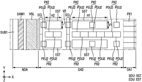
1. A display device comprising:
a substrate including a first display region and a second display region surrounding the first display region;
a first pixel disposed in the first display region;
a second pixel disposed in the second display region; and
a scan driver including scan stages which are disposed in the second display region and apply scan signals to the first pixel and the second pixel, each of the scan stages being connected to a scan line extending along a first direction,
wherein the first pixel includes a first pixel driver including a first pixel transistor and a first pixel light-emitting device connected to the first pixel driver, the second pixel includes a second pixel driver including a second pixel transistor and a second pixel light-emitting device connected to the second pixel driver, and
wherein the second pixel driver is disposed between scan stages adjacent to each other along a second direction crossing the first direction.
|