| CPC G09G 3/3258 (2013.01) [G09G 3/3266 (2013.01); G09G 2300/0426 (2013.01)] | 20 Claims |
|
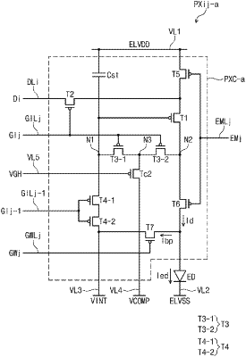
1. A pixel comprising:
a capacitor electrically connected between a first voltage line and a first node, the first voltage line being configured to receive a first voltage;
a light emitting diode comprising a first electrode electrically connected to a second node, and a second electrode electrically connected to a second voltage line;
a first transistor comprising a first electrode electrically connected to the first voltage line, a second electrode connected to the second node, and a gate electrode electrically connected to the first node;
a second transistor comprising a first electrode connected to a data line, a second electrode electrically connected to the first electrode of the first transistor, and a gate electrode configured to receive a first scan signal;
a third transistor comprising a first electrode electrically connected to the first node, a second electrode electrically connected to the second node, and a gate electrode configured to receive the first scan signal;
a fourth transistor comprising a first electrode electrically connected to the first node, a second electrode electrically connected to a third voltage line configured to receive a third voltage, and a gate electrode configured to receive a second scan signal; and
a compensation transistor different from the third transistor and forming a current path between the first node and a fourth voltage line configured to receive a compensation voltage, the compensation transistor comprising a first electrode electrically connected to the first node, a second electrode electrically connected to the fourth voltage line, and a gate electrode configured to receive a compensation control voltage.
|