| CPC G09G 3/3241 (2013.01) [G09G 3/3266 (2013.01); G09G 3/3291 (2013.01); G09G 2300/0876 (2013.01)] | 9 Claims |
|
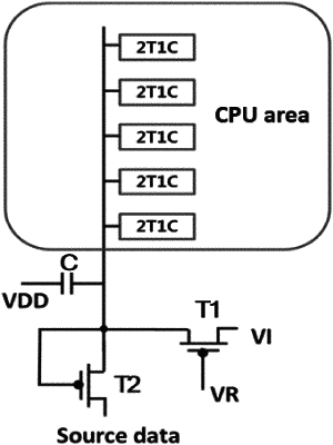
1. A pixel circuit, comprising:
a data line configured to transmit a source data signal;
a scan line configured to transmit a scan signal;
a plurality of hierarchical 2 transistors and 1 storage capacitor (2T1C) circuits, each input thereof is connected to the scan line in parallel;
a step-down circuit comprising an input connected to the data line and an output connected to the input of each 2T1C circuit;
a reset circuit connected to the output of the step-down circuit; and
a voltage stabilizing capacitor comprising an end electrically connected to a positive power supply voltage and another end electrically connected to the input of the 2T1C circuit, wherein the voltage stabilizing capacitor is configured to stabilize a voltage input to the 2T1C circuit.
|