| CPC G09G 3/3233 (2013.01) [G09G 3/3266 (2013.01); H10K 59/1213 (2023.02); H10K 59/1216 (2023.02); H10K 59/131 (2023.02); G09G 2300/0426 (2013.01); G09G 2300/0819 (2013.01); G09G 2300/0852 (2013.01); G09G 2310/08 (2013.01); G09G 2320/0247 (2013.01); G09G 2330/021 (2013.01); H01L 27/124 (2013.01); H01L 27/1225 (2013.01); H01L 27/1251 (2013.01); H01L 27/1255 (2013.01); H01L 29/7869 (2013.01); H01L 29/78675 (2013.01)] | 20 Claims |
|
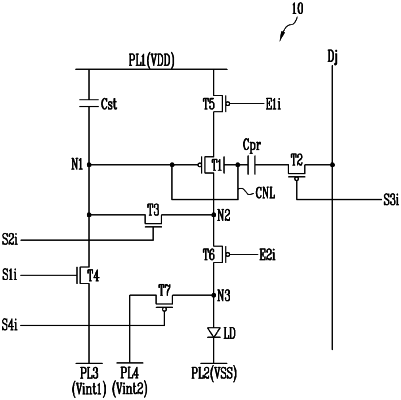
1. A pixel comprising:
a light-emitting element;
a first transistor which generates a driving current which flows from a first power line which provides a first power voltage to a second power line which provides a second power voltage through the light-emitting element, the first transistor comprising a first gate electrode and a second gate electrode;
a second transistor which is connected between a data line and the second gate electrode of the first transistor, and turned on in response to a third scan signal supplied to a third scan line;
a third transistor which is connected between a first node connected to the first gate electrode of the first transistor and a second node, and turned on in response to a second scan signal supplied to a second scan line;
a fourth transistor which is connected between the first node and a third power line, provides a third power voltage, and turned on in response to a first scan signal supplied to a first scan line;
a fifth transistor which is connected between the first power line and the first transistor, and turned off in response to a first emission control signal supplied to a first emission control line;
a sixth transistor which is connected between a third node connected to an electrode of the light-emitting element and the second node, and turned off in response to a second emission control signal supplied to a second emission control line; and
a first capacitor connected between the first power line and the first node.
|