| CPC G09G 3/3233 (2013.01) [G09G 2300/0426 (2013.01); G09G 2300/0819 (2013.01); G09G 2300/0852 (2013.01); G09G 2310/0262 (2013.01); G09G 2310/08 (2013.01); G09G 2320/0209 (2013.01); G09G 2320/0233 (2013.01)] | 17 Claims |
|
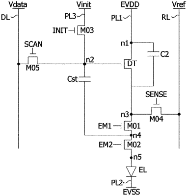
1. A pixel circuit comprising:
a driving element including a first electrode connected to a first node to which a pixel driving voltage is applied, a gate electrode connected to a second node, and a second electrode connected to a third node;
a first switch element including a first electrode connected to the third node, a gate electrode to which a first light emission control pulse is applied, and a second electrode connected to a fourth node;
a second switch element including a first electrode connected to the fourth node, a gate electrode to which a second light emission control pulse is applied, and a second electrode connected to a fifth node;
a light emitting device including an anode connected to the fifth node, and a cathode electrode to which a low potential power voltage is applied;
a first capacitor connected between the second node and the fourth node; and
a second capacitor connected between the first node and the third node.
|