US 11,727,877 B2
Pixel preventing leakage current and display device using the same
Young-In Hwang, Suwon-si (KR); Sung Ho Kim, Suwon-si (KR); Eung Taek Kim, Hwaseong-si (KR); Yong Ho Yang, Suwon-si (KR); Seong Min Wang, Seongnam-si (KR); and Jung-Mi Choi, Seoul (KR)
Assigned to Samsung Display Co., Ltd., Yongin-si (KR)
Filed by Samsung Display Co., Ltd., Yongin-Si (KR)
Filed on Aug. 19, 2022, as Appl. No. 17/891,877.
Application 17/891,877 is a continuation of application No. 17/157,768, filed on Jan. 25, 2021, granted, now 11,423,835.
Application 17/157,768 is a continuation of application No. 16/285,080, filed on Feb. 25, 2019, granted, now 10,902,774, issued on Jan. 26, 2021.
Claims priority of application No. 10-2018-0027043 (KR), filed on Mar. 7, 2018.
Prior Publication US 2022/0392405 A1, Dec. 8, 2022
This patent is subject to a terminal disclaimer.
Int. Cl. G09G 3/3233 (2016.01); G09G 3/3291 (2016.01); G09G 3/3266 (2016.01); G09G 3/3258 (2016.01); H10K 59/131 (2023.01)
CPC G09G 3/3233 (2013.01) [G09G 3/3258 (2013.01); G09G 3/3266 (2013.01); G09G 3/3291 (2013.01); H10K 59/131 (2023.02); G09G 2300/0426 (2013.01); G09G 2300/0809 (2013.01); G09G 2320/0214 (2013.01)] 20 Claims
OG exemplary drawing
 
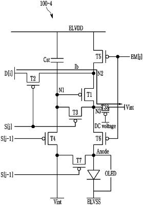
1. A pixel comprising:
an organic light emitting diode;
a first transistor including a gate that is connected to a first node, wherein the first transistor is connected between a second node and a third node;
a second transistor including a gate that is connected to a corresponding scan line, wherein the second transistor is connected between a data line and the second node;
a storage capacitor connected between the first node and a first voltage;
a third transistor including a gate that is connected to the corresponding scan line, wherein the third transistor is connected between the first node and the third node; and
a fourth transistor connected between a drain of the first transistor and a first DC voltage supply source having a voltage value of a gate-off level.