| CPC G09G 3/3233 (2013.01) [G06V 10/143 (2022.01); G06V 40/1318 (2022.01); G09G 3/2003 (2013.01); G06F 3/0446 (2019.05); G09G 2300/0452 (2013.01); G09G 2300/0809 (2013.01); G09G 2354/00 (2013.01)] | 15 Claims |
|
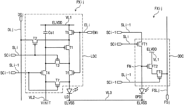
1. A display panel, comprising:
a light emitting pixel comprising a light emitting element including a first electrode and a second electrode, and a plurality of transistors; and
a light sensing pixel comprising a photo sensor including a first electrode and a second electrode, and a plurality of transistors,
wherein one of the plurality of transistors of the light emitting pixel is electrically connected to a scan line,
wherein the second electrode of the light emitting element and the second electrode of the photo sensor have an integral shape,
wherein the plurality of transistors of the light emitting pixel comprise:
a first transistor including a first electrode, a second electrode and a gate electrode;
a second transistor including a first electrode connected to the first electrode of the first transistor, a second electrode connected to a data line and a gate electrode connected to a first scan line; and
a third transistor including a first electrode connected to the second electrode of the first transistor, a second electrode connected to the gate electrode of the first transistor and a gate electrode connected to the first scan line,
wherein the plurality of transistors of the light sensing pixel comprise a reset transistor including a first electrode, a second electrode and a gate electrode directly connected to the first scan line.
|