| CPC G09G 3/3233 (2013.01) [H01L 27/1225 (2013.01); G09G 3/3275 (2013.01); G09G 2300/0465 (2013.01); G09G 2310/0291 (2013.01); G09G 2320/0252 (2013.01); G09G 2320/041 (2013.01); G09G 2330/021 (2013.01); H10K 59/12 (2023.02)] | 7 Claims |
|
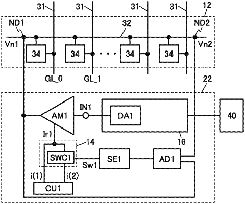
1. A semiconductor device comprising:
a signal line comprising a first node and a second node;
a plurality of pixels electrically connected to the signal line and positioned between the first node and the second node;
an analog-to-digital converter circuit electrically connected to the first node and the second node;
a sensing circuit electrically connected to the analog-to-digital converter circuit; and
an amplifier circuit electrically connected to the first node and supplied with an image signal,
wherein the analog-to-digital converter circuit is configured to convert a potential of the first node into a first signal, and to convert a potential of the second node into a second signal,
wherein the sensing circuit is configured to generate a third signal by a comparison result of the first signal and the second signal, and
wherein the amplifier circuit is configured to amplify the image signal in accordance with the third signal, and to output an amplified image signal to the first node.
|