| CPC G09G 3/3233 (2013.01) [H10K 59/1213 (2023.02); H10K 59/131 (2023.02); G09G 2300/0426 (2013.01); G09G 2300/0809 (2013.01); G09G 2320/0209 (2013.01); H10K 59/126 (2023.02)] | 26 Claims |
|
1. A pixel circuit, comprising:
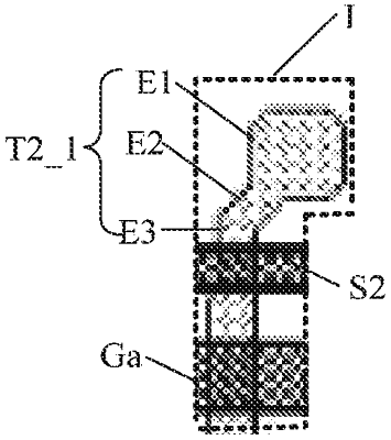
a threshold compensation transistor, an active layer of the threshold compensation transistor comprises a first channel portion, a second channel portion, and a connection portion between the first channel portion and the second channel portion;
a shielding element coupled to a first power line, the shielding element comprises a first shielding portion and a second shielding portion coupled with each other, and an orthographic projection of the first shielding portion on a substrate is overlapped with an orthographic projection of the connection portion on the substrate;
a data writing transistor, a gate of the data writing transistor being coupled to a gate line, a first electrode of the data writing transistor being coupled to a data line, the gate line extending in a first direction, the data line extending in a second direction intersecting the first direction, an orthographic projection of an active layer of the data writing transistor on the substrate being overlapped with an orthographic projection of the gate line on the substrate to form a first overlapping area; the first electrode of the data writing transistor and the active layer are located in a same layer, and an orthographic projection of the first electrode of the data writing transistor on the substrate is overlapped with an orthographic projection of the second shielding portion on the substrate to form a second overlapping area; a size of the second overlapping area in the first direction is smaller than a size of the first overlapping area in the first direction.
|