| CPC G09G 3/3233 (2013.01) [G09G 3/3266 (2013.01); H10K 59/1213 (2023.02); H10K 59/1216 (2023.02); H10K 59/131 (2023.02); H10K 59/1315 (2023.02); G09G 2300/0426 (2013.01); G09G 2300/0819 (2013.01); G09G 2300/0842 (2013.01); G09G 2300/0861 (2013.01); G09G 2300/0866 (2013.01); G09G 2320/0233 (2013.01); H10K 59/1201 (2023.02)] | 20 Claims |

|
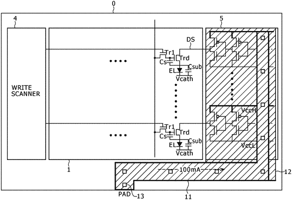
1. A display device comprising:
a first wire;
a second wire;
a plurality of contacts; and
an insulating film,
wherein:
the insulating film is disposed, in a cross sectional view of the display device, between the first wire and the second wire,
each of the contacts extends through the insulating film from the first wire to the second wire,
a first one of the contacts, in a plan view of the display device, is disposed along a row direction between a second one of the contacts and a third one of the contacts, and
a fourth one of the contacts, in the plan view of the display device, is disposed along an axis extending in a column direction between the third one of the contacts and a fifth one of the contacts.
|