| CPC G09G 3/3225 (2013.01) [G09G 3/3233 (2013.01); H10K 59/12 (2023.02); G09G 2300/0819 (2013.01); G09G 2300/0842 (2013.01); G09G 2300/0861 (2013.01); G09G 2310/08 (2013.01); G09G 2320/0214 (2013.01); G09G 2320/0233 (2013.01); G09G 2320/0247 (2013.01); G09G 2320/04 (2013.01); G09G 2320/045 (2013.01); G09G 2320/0626 (2013.01); G09G 2330/021 (2013.01)] | 20 Claims |
|
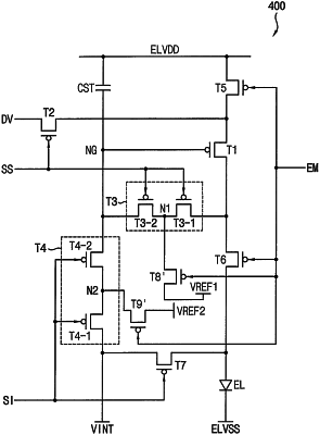
1. A pixel of a display device, the pixel comprising:
a capacitor including a first electrode coupled to a line of a first power supply voltage, and a second electrode coupled to a gate node;
a first transistor including a gate coupled to the gate node;
a second transistor which transfers a data voltage to a source of the first transistor in response to a first signal;
a third transistor which diode-connects the first transistor in response to the first signal, wherein the third transistor includes first and second sub-transistors which are coupled to each other in series between a drain of the first transistor and the gate node;
a fourth transistor which applies a first initialization voltage to the gate node in response to a second signal, wherein the fourth transistor includes third and fourth sub-transistors which are coupled to each other in series between a line of the first initialization voltage and the gate node;
a fifth transistor which couples the line of the first power supply voltage and the source of the first transistor in response to a third signal;
a sixth transistor which couples the drain of the first transistor and an anode of a light emitting element in response to the third signal;
an eighth transistor which applies a first reference voltage to a first node between the first and second sub-transistors in response to the third signal;
a ninth transistor which applies a second reference voltage different from the first reference voltage to a second node between the third and fourth sub-transistors in response to the third signal; and
the light emitting element including the anode, and a cathode coupled to a line of a second power supply voltage.
|