| CPC G09G 3/32 (2013.01) [G09G 3/2074 (2013.01); G09G 2300/0408 (2013.01); G09G 2300/0426 (2013.01); G09G 2300/0443 (2013.01); G09G 2300/0452 (2013.01); G09G 2300/0804 (2013.01); G09G 2310/0208 (2013.01); G09G 2310/0278 (2013.01)] | 10 Claims |
|
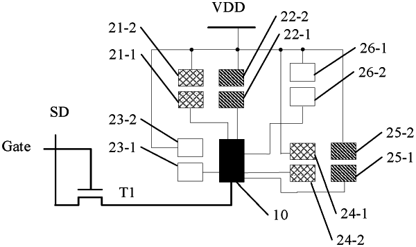
1. A pixel drive circuit, comprising a switch unit and a drive unit, wherein the switch unit is connected to the drive unit, and the drive unit is configured to be connected to a plurality of sub-pixel units;
the switch unit is configured to receive a scan signal and a data signal, be switched on under action of the scan signal, and send the data signal to the drive unit; and
the drive unit is configured to send the data signal to the plurality of sub-pixel units connected thereto in a time division manner;
wherein six sub-pixel units are provided, the six sub-pixel units comprise a first sub-pixel unit, a second sub-pixel unit, a third sub-pixel unit, a fourth sub-pixel unit, a fifth sub-pixel unit, and a sixth sub-pixel unit; and
the sub-pixel units and the drive unit are arranged in two rows and four columns, the first sub-pixel unit, the second sub-pixel unit, and the sixth sub-pixel unit are located in a first row side by side, and the third sub-pixel unit, the drive unit, the fourth sub-pixel unit, and the fifth sub-pixel unit are located in a second row side by side.
|