| CPC G09G 3/2092 (2013.01) [G09G 2300/0426 (2013.01); G09G 2310/0275 (2013.01)] | 21 Claims |
|
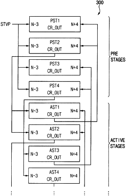
1. A gate driver comprising:
a plurality of active stages configured to output gate signals to a display part; and
a plurality of pre-stages, connected to the active stages, configured to output carry signals to the active stages,
wherein the pre-stages do not output the gate signals to the display part,
wherein the pre-stages include a first pre-stage and a second pre-stage,
wherein, among the active stages and the pre-stages, only the second pre-stage includes a Q node compensator configured to receive a clock signal from the first pre-stage and to compensate for a voltage of a Q node based on the clock signal of the first pre-stage,
wherein the Q node compensator includes a feedback transistor configured to diode-connect a feedback input terminal, which is configured to receive the clock signal of the first pre-stage, to a feedback node of the second pre-stage.
|